
Products
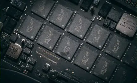
Mobile Mainboard Design & High-Density Assembly
At Quon Electronics LLP, we deliver precision engineering, high-density SMT assembly, and comprehensive testing for complex smartphone mainboards, wearables, and compact edge devices. From ultra-fine pitch component placement to multi-layer High-Density Interconnect (HDI) layout optimization, our manufacturing lines are equipped to build robust, high-performance mainboards engineered for space-constrained applications.
Technical Capabilities
- Micro-BGA & Fine-Pitch SMT Assembly: Automated placement of 01005 passives, Package-on-Package (PoP) architectures, and fine-pitch ICs with sub-micron alignment accuracy.
- Advanced HDI Multi-Layer Stackups: Up to 12+ layer board fabrication utilizing laser microvias, stacked/staggered blind and buried vias, and high-density signal trace routing.
- RF & High-Speed Signal Routing: Multi-band RF front-end routing engineered for 4G/5G NR, Wi-Fi 6/6E, Bluetooth, GPS, and NFC modules with minimal cross-talk and stray impedance.
- Thermal Management & EMI Shielding: Automated placement of metal shielding cans (RF cans), thermal graphite sheets, and phase-change thermal interface materials for processor cooling under high workloads.
- Power Management Optimization: Efficient trace routing and plane design for multi-rail PMICs, fast-charging protocols, and extended battery endurance.
Manufacturing & Quality Specifications
| Capability / Metric | Technical Standard |
|---|---|
| Substrate Thickness | Ultra-thin substrates (0.4mm – 0.8mm), High-Tg FR-4 / Polyimide |
| Inspection Standards | 3D Solder Paste Inspection (SPI) & 3D Automated Optical Inspection (AOI) |
| BGA Solder Inspection | 3D X-Ray Inspection (AXI) for micro-voiding and solder joint validation |
| Testing Protocols | Boundary scan, flying probe, custom functional test rigs, and RF calibration |
| Quality Compliance | ISO 9001:2015, IPC-A-610 Class 3, RoHS Lead-Free |